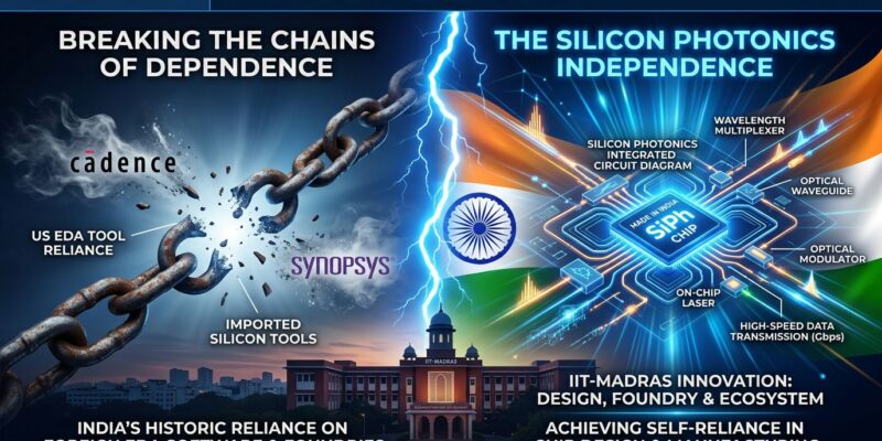
India’s Ministry of Electronics and IT launched the country’s first indigenous Silicon Photonics Process Design Kit on April 24 at IIT-Madras, breaking decades of dependence on US-controlled chip design tools. The toolkit includes a PDK with 50+ verified components and an automated test engine—everything needed to design photonic integrated circuits without touching Cadence or Synopsys software. Timing couldn’t be better: Nvidia just made silicon photonics mandatory for next-gen AI data centers, and India now has domestic tools ready as that $50 billion market explodes.
Why Silicon Photonics Matters for AI Infrastructure
Silicon photonics replaces copper interconnects with light, delivering 100x faster data transfer at 70% less power. Nvidia’s 2026 Quantum-X switches use photonic interconnects to hit 115 Tb/s throughput—critical for AI workloads where GPUs constantly shuttle training data between memory and processors. Every ChatGPT query, Claude conversation, and Gemini response depends on terabit-scale data movement. Copper can’t keep up.
Moreover, the market sees it. IDTechEx forecasts photonic integrated circuits hitting $50 billion by 2036, with a 21.9% compound annual growth rate driven almost entirely by AI data centers. India didn’t build tools for yesterday’s technology—they’re positioning for the infrastructure wave that’s already cresting.
What IIT-Madras Actually Built
The Silicon Photonics PDK contains 50+ building-block components for designing photonic chips. That’s smaller than Cadence or Synopsys libraries (which have thousands), but it’s enough for research, defense prototypes, and startup MVPs. More importantly, it’s free for Indian users and doesn’t come with US export restrictions. Defense labs can now design secure photonic systems without sending blueprints through foreign software.
Additionally, the Universal PPIC Test Engine eliminates another chokepoint: overseas testing. Previously, Indian researchers had to ship designs abroad for characterization—slow, expensive, and a security nightmare for defense applications. Now they test locally at IIT-Madras. Starting Q3 FY2026-27, the center will offer Multi-Project Wafer fabrication runs through SilTerra Malaysia, letting multiple teams share wafer costs. Consequently, a startup can prototype a photonic chip for a fraction of what Cadence licenses cost annually.
India’s Smart Play vs China’s Brute Force
Compare India’s approach to China’s semiconductor self-sufficiency push. China threw $47.5 billion at semiconductor funds and is burning another $47 billion on wafer fab equipment in 2026, trying to replicate TSMC despite ASML’s EUV lithography ban. Result: SMIC limping along with less efficient DUV tools, struggling to hit 7nm yields, stuck at ~16% self-sufficiency after years of effort.
India chose different battles. Instead of fighting US sanctions head-on at cutting-edge nodes, they’re targeting strategic niches where capital requirements are lower and partnerships work. Silicon photonics for AI and quantum applications. Design talent over fab infrastructure (leveraging India’s existing software expertise). SilTerra Malaysia for fabrication instead of building domestic fabs that might never materialize. India Semiconductor Mission 2.0 budgeted ₹8,000 crore ($960M)—pocket change compared to China’s spending—but focused on 24 design startups, 62,000 trained engineers, and ATMP/OSAT facilities rather than chasing 2nm dreams.
Clearly, it’s smarter positioning. Photonics is becoming mandatory for AI infrastructure (Nvidia’s roadmap proves it), India has tools ready, and they avoided the capital-intensive fab trap that’s killed previous Indian semiconductor initiatives.
Execution Risk: History Says Be Skeptical
India has a graveyard of failed semiconductor ambitions. Multiple fab proposals in the 2000s and 2010s collapsed after grand announcements. Coordination between government, academia, and industry repeatedly broke down. Betting on cutting-edge nodes was always unrealistic.
So why believe this time? Three reasons. First, focused scope: they’re not trying to build bleeding-edge fabs, just design tools and partnerships for strategic niches. Second, the partnership model with SilTerra Malaysia reduces capital risk—India isn’t going it alone. Third, timing: the global chip shortage and AI boom created real urgency and actual funding (₹8,000 crore for ISM 2.0 vs past token commitments).
However, risks remain. The 50-component PDK library needs years of expansion to match foreign tools. The SilTerra Malaysia partnership is a single point of failure for fabrication. Izmo Microsystems is the only domestic packaging option. Furthermore, there’s a massive gap between “academic PDK for research” and “production-ready commercial tools.” India targets 70-75% domestic chip capability by 2029 and top semiconductor nation status by 2035—ambitious timelines given past performance.
But here’s the realistic take: this PDK won’t replace Cadence or Synopsys for commercial production anytime soon. It doesn’t have to. Success means defense labs can design secure photonic systems domestically, startups can prototype without six-figure licenses, and universities can train the next generation of chip designers. That’s strategic autonomy where it counts, even if India never matches Silicon Valley’s commercial ecosystem.
Execution will determine if this is India’s semiconductor breakthrough or another false start. The tools exist, the partnerships are signed, and the timing is right. Now comes the hard part: actually delivering.