 By ByteBot
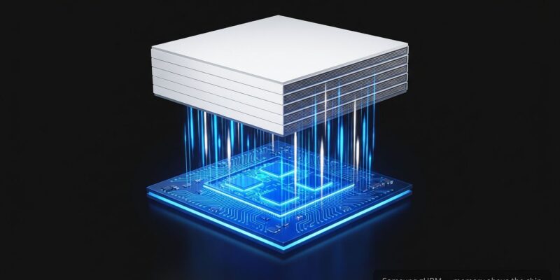
Samsung just told the AI industry that side-by-side memory is a dead end. At FMS 2026 this week, the company unveiled zHBM — a next-generation memory architecture that stacks high-bandwidth memory directly on top of AI accelerators, not beside them. The claim: 8x the bandwidth of HBM5, 10x the density, 3x the energy efficiency. The honest caveat: it is a concept, and it will not ship before 2028 at the earliest. That gap matters less than you might think.
From Beside to Above: What zHBM Actually Does
Current HBM — including the HBM5 in today’s flagship accelerators — sits laterally alongside the GPU die. Data travels horizontally between compute and memory. It works, but every nanosecond of transit is a nanosecond of latency, and at the token generation speeds the industry needs, those nanoseconds add up.
zHBM eliminates the horizontal trip. Using wafer-bonding techniques, Samsung stacks memory layers directly above the compute die along the Z-axis. The signal path collapses. The result, if the specs hold: bandwidth that makes HBM5 look like DDR4 by comparison — 8x the throughput, over 10x the density in the same physical footprint, and thermal resistance cut by more than half.
Samsung is also building space for customer-specific IP integration between the memory and compute layers. That means enterprises like Google, Meta, and OpenAI could theoretically bake workload-specific optimizations directly into the memory-accelerator interface — turnkey custom silicon, with Samsung handling memory, foundry, and packaging as a single vendor.
Why Memory Bandwidth Is the Real Bottleneck
If you have ever watched an inference benchmark and wondered why throwing more GPUs at the problem does not scale linearly, memory bandwidth is probably why. During the decode phase — when a model generates tokens one by one — model weights are read from memory and used once per token. The compute sits idle waiting for data to arrive. You are not compute-bound. You are bandwidth-bound.
Put numbers on it: a 70B parameter model at FP16 requires roughly 140 GB of data moved per token step. The NVIDIA B200, with its 8 TB/s HBM3e bandwidth, handles that in about 17.5 milliseconds at theoretical maximum — and real-world numbers are worse. Scale to production workloads with concurrent sessions and long KV caches, and the wall becomes visible in your latency graphs and your cloud bill. The memory wall is well-documented at this point: adding GPUs does not reduce latency when you are memory-bound.
zHBM’s 8x bandwidth multiplier — applied against a future accelerator with HBM5 as the base — would put theoretical bandwidth somewhere north of 60 TB/s. That same 70B model decode drops to low single-digit milliseconds. Context windows past a million tokens without thrashing memory become tractable. It is a different class of machine.
What Samsung Actually Announced at FMS 2026
zHBM was the headline, but FMS 2026 included several announcements with shorter runways to production.
- V10 BV-NAND — Samsung’s first wafer-bonded NAND architecture, crossing 400 layers and delivering a 58% density increase over V9. Improved read, write, and I/O performance included. Potential 2027 availability.
- LPDDR5X-PIM — Industry-first LPDDR memory with processing-in-memory capability. Reduces data movement between processor and memory, which is the root cause of the memory wall. Closer to shipping than zHBM.
- zNAND-O — Four-layer and eight-layer NAND targeting edge AI environments, optimized for real-time inference with low latency and high I/O in a small form factor.
- HBM roadmap status — HBM4 entered mass production February 2026, HBM4E samples shipped globally in May, HBM5 is in full production now.
StorageReview’s full FMS 2026 breakdown covers the complete roadmap for those who want the unabridged version.
The Honest Take: Concept Is Not a Shipping Date
zHBM has no announced production timeline, no pricing, and no confirmed compatibility with Nvidia or AMD accelerator platforms. HBM4 — two generations behind zHBM — is not even broadly deployed commercially yet. Samsung is showing the industry where memory is headed, not handing out purchase orders.
That is fine. Roadmap signals matter. If you are architecting AI infrastructure for the next three to five years, you should assume memory bandwidth will increase by an order of magnitude. That means model sizes, quantization strategies, and context window assumptions built against today’s 8 TB/s ceiling may look conservative when zHBM-class systems arrive. Design with that trajectory in mind.
For the next 12 to 18 months, the practical story is HBM4E, LPDDR5X-PIM, V10 BV-NAND, and whatever SK Hynix ships with its HBF hybrid architecture. Those are the bandwidth numbers your infrastructure planning should use today. zHBM is the direction — not the destination.
The Bottom Line
Samsung’s zHBM announcement is part of a broader pattern: every major hardware player in 2026 is attacking the compute-memory gap from a different angle. AMD is etching weights into silicon ROM-style via the Taalas acquisition. SK Hynix is combining HBM and HBF in hybrid stacks. Samsung is moving memory on top of the chip entirely. None of these are products you can order today, but they all point in the same direction.
The memory wall is real, measurable in inference latency, and the industry knows it. That Samsung felt the need to drop an 8x performance headline at FMS 2026 tells you how acute the pressure has become. The developers who understand that memory bandwidth — not GPU FLOPS — is the actual constraint will make better infrastructure decisions in the years between now and when zHBM ships.